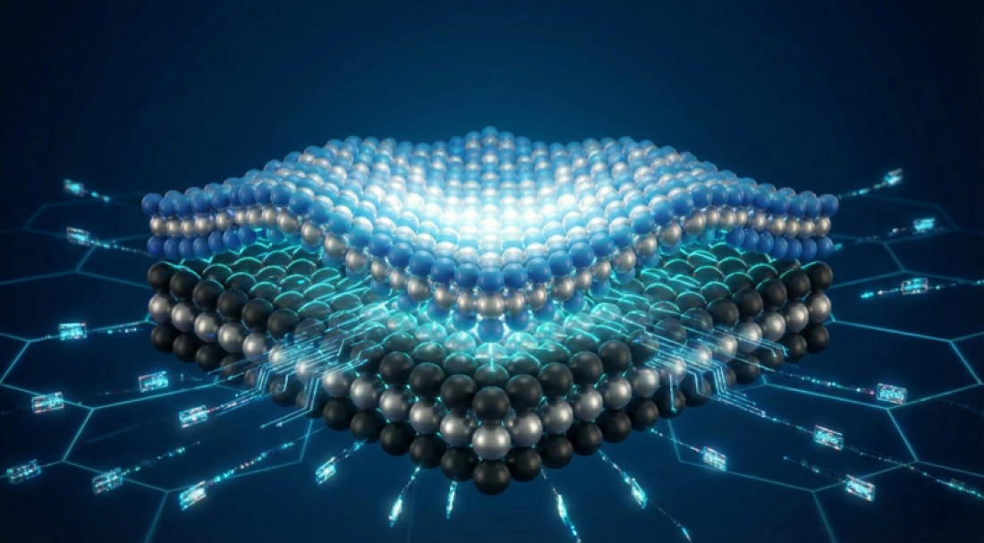
At the atomic scale, stacking two-dimensional (2D) materials into so-called van der Waals (vdW) heterostructures can generate physical properties absent in their bulk forms. Although held together only by weak interlayer forces, the close proximity of distinct atomic layers can profoundly reshape their electronic landscape through charge redistribution and orbital hybridization.
What happens when two quantum materials are stacked together layer by layer? A team led by Professor Jyh-Pin Chou at National Taiwan University and Professor Meng-Kai Lin at National Central University has shown that moiré-modulated interfaces in PtSe2/PtTe2 heterostructures can fundamentally reshape their electronic band structures.
Both PtSe2 and PtTe2 are Dirac semimetals in their bulk, three-dimensional forms. However, when thinned down to only a few atomic layers, they transition into semiconductors due to dimensional confinement. The researchers set out to understand what happens when these two materials are vertically combined—how does their mutual interaction reconstruct their electronic behavior?
To address this question, Professor Chou’s team performed systematic first-principles calculations based on density functional theory (DFT) to reveal the underlying microscopic mechanisms, while Professor Lin’s team grew high-quality single-crystalline films using molecular beam epitaxy and directly mapped their electronic band dispersions with angle-resolved photoemission spectroscopy.
“The key lies in the geometry and moiré modulation at the interface,” the team explains. Their calculations reveal that periodic interlayer interactions induce microscopic structural distortions, specifically a buckling of the PtSe2 layer. This distortion originates from the moiré pattern formed when two atomic lattices with slightly different periodicities overlap.
Importantly, this structural buckling breaks inversion symmetry. When combined with the strong spin–orbit coupling inherent to heavy elements such as platinum, the symmetry breaking produces a pronounced spin-dependent band splitting. Such spin splitting is highly relevant for spintronic applications, where electronic spin, rather than charge alone, is used to encode and manipulate information.
Further analysis of the local density of states revealed that electronic properties vary dramatically across different stacking regions of the moiré superlattice. Some regions exhibit metallic behavior, while others remain semiconducting with band gaps of 0.40 eV and 0.25 eV. This spatial modulation demonstrates how interfacial stacking alone can create electronically distinct domains within a single atomic interface.
One of the most striking discoveries was the emergence of flat-band features near the Fermi level. Flat bands indicate strong electron localization within specific regions of the moiré lattice. Such localization is widely regarded as a potential precursor to correlated electron phenomena, including unconventional superconductivity and other emergent quantum states.
By experimentally and theoretically demonstrating that moiré-induced structural distortions can control spin splitting, hybridization strength, and electron localization, the team establishes PtSe2/PtTe2 heterostructures as a model platform for exploring interface-driven quantum phenomena.
“Our findings deepen our understanding of how interfacial interactions and moiré modulation govern the electronic landscape of 2D systems,” says co-corresponding author Professor Jyh-Pin Chou.
“This opens new possibilities for rationally designing next-generation low-dimensional quantum and spintronic devices.”
Prof. Jyh-Pin Chou's email address: jpchou@ntu.edu.tw
To see article on Asia Research News: https://www.asiaresearchnews.com/content/moir%C3%A9-induced-electronic-reconstruction-van-der-waals-heterobilayer-ptse2ptte2